
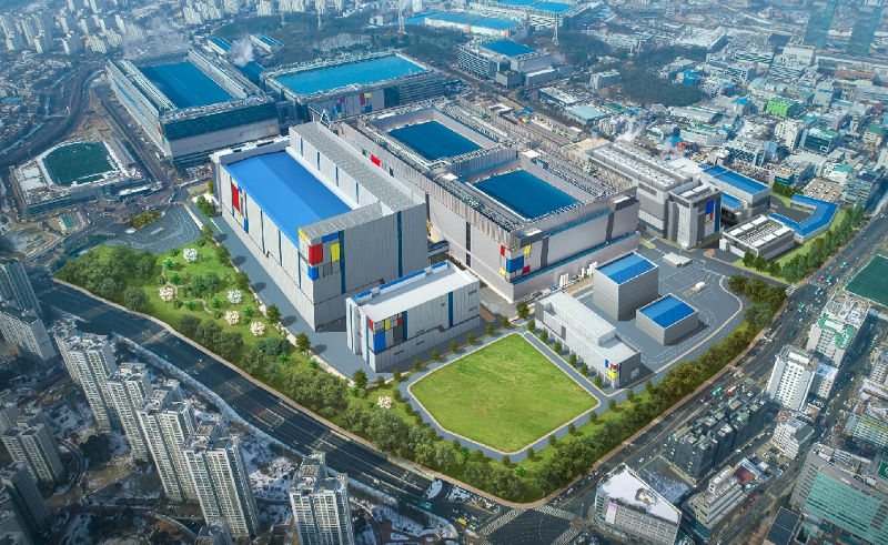
 Samsung back in September last year announced that it is working on 7LPP (Low Power Plus) with EUV (extreme ultra violet) lithography technology for smartphones that is targeted for initial production in the second half of 2018. Earlier this Feburary it announced that it is building new EUV (extreme ultraviolet) line in Hwaseong, Korea. Earlier this week the company started wafer production of its revolutionary process node, 7LPP, the 7-nanometer (nm) LPP (Low Power Plus) with extreme ultraviolet (EUV) lithography technology. The EUV system, which utilizes extreme ultraviolet technology, can perform photolithography process by using a light source with EUV wavelength. In the world of chip manufacturing, realizing finer circuits is vital as it enables integration of more components inside a chip, which helps build those with higher power and energy efficiency. Upcoming EUV scanners will utilize EUV radiation at a 13.5nm wavelength, less than 1/14 of what current ArF excimer laser scanners are able to provide. EUV uses 13.5nm wavelength light to expose silicon wafers as opposed to conventional argon fluoride (ArF) immersion technologies that are only able to achieve 193nm wavelengths and require expensive multi-patterning mask sets. EUV enables the use of a single mask to create a silicon wafer layer where ArF can ...
Read Here»
Post a Comment Blogger Facebook
We welcome comments that add value to the discussion. We attempt to block comments that use offensive language or appear to be spam, and our editors frequently review the comments to ensure they are appropriate. As the comments are written and submitted by visitors of The Sheen Blog, they in no way represent the opinion of The Sheen Blog. Let's work together to keep the conversation civil.