
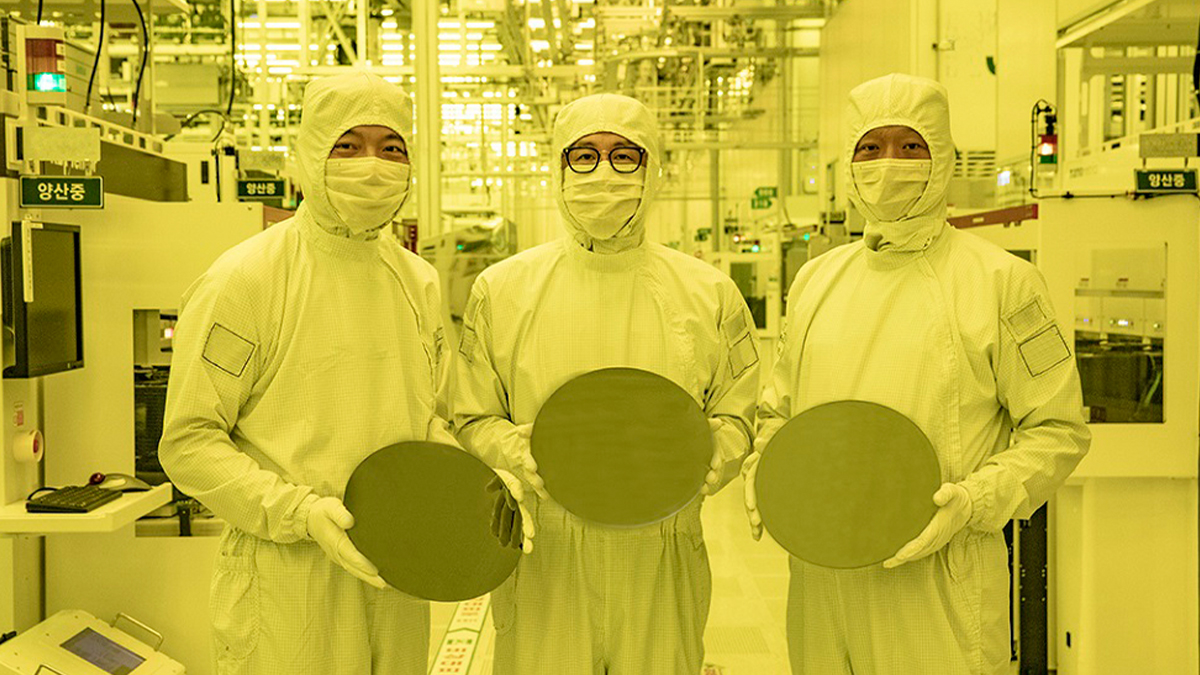
Today, Samsung Electronics revealed that production of its 3-nanometer (nm) manufacturing node using the Gate-All-Around (GAA) transistor architecture has begun. The company said that when matched to its 5nm process, their 3nm process consumes 45% less power, offers improved performance by 23%, and has a 16% smaller surface area. Samsung’s 3nm process node incorporates a … Continue reading "Samsung begins production of world’s first 3nm chips"
The post Samsung begins production of world’s first 3nm chips first appeared on Fone Arena.
Read Here»
Post a Comment Blogger Facebook
We welcome comments that add value to the discussion. We attempt to block comments that use offensive language or appear to be spam, and our editors frequently review the comments to ensure they are appropriate. As the comments are written and submitted by visitors of The Sheen Blog, they in no way represent the opinion of The Sheen Blog. Let's work together to keep the conversation civil.