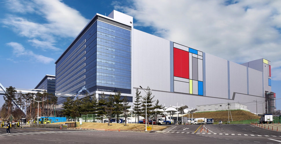
 Samsung today announced that it has opened new V1 semiconductor fabrication line in Hwaseong, Korea, dedicated to the extreme ultraviolet (EUV) lithography technology and produces chips using process node of 7 nanometer (nm) and below. It started building it back in February 2018, and began test wafer production in the second half of 2019. The V1 line is currently producing state-of-the-art mobile chips with 7 and 6nm process technology, and the company said that it will continue to adopt finer circuitry up to the 3nm process node. Samsung already said that the cumulative total investment in the V1 line will reach US$6 billion by the end of 2020, and the total capacity from 7nm and below process node is expected to triple from that of 2019. Together with the S3 line, the V1 line is expected to play a pivotal role in responding to fast-growing global market demand for single-digit node foundry technologies. “As semiconductor geometries grow smaller, the adoption of EUV lithography technology has become increasingly important, as it enables scaling down of complex patterns on wafers and provides an optimal choice for next-generation applications such as 5G, AI, and Automotive,” said Samsung. With the V1 line in operation, Samsung now has ...
Read Here»

Post a Comment Blogger Facebook
We welcome comments that add value to the discussion. We attempt to block comments that use offensive language or appear to be spam, and our editors frequently review the comments to ensure they are appropriate. As the comments are written and submitted by visitors of The Sheen Blog, they in no way represent the opinion of The Sheen Blog. Let's work together to keep the conversation civil.